
A conceptually simple passive component is used to combine or split DC and RF signals; however, its implementation has many subtleties.
The RF world, operating at hundreds of megahertz and into the gigahertz range, is known for having many unusual components. Some are unique to that higher-frequency world, while others appear at lower frequencies but with different component sizes and physical construction.
The bias tee (occasionally written as bias-T) is a widely used RF component that is also sometimes used at lower frequencies. This FAQ will examine the function of the bias tee and issues related to its design and construction.
Q: What is a bias tee, and what does it do?
A: The bias tee is a passive, bidirectional device. It must have complementary uses: to combine DC power and high-frequency (RF) signals into a single port (RF and DC) or to split a combined RF and DC signal into its two constituents. It is also called a power combiner or power splitter, but that downplays its RF aspects. Note that some vendors confusingly call the RF signal an AC signal to contrast it with DC power, but it is an RF signal, not a power-line AC.
Q: What does the basic schematic diagram of a bias tee look like?
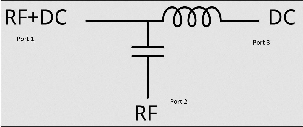
A: It is a three-port device with just two passive components: a DC-blocking capacitor and an RF-blocking inductor (often called a choke), shown in Figure 1.
Figure 1. The bias tee has a very simple schematic diagram, in principle. (Image: Wikipedia)
Q: How does it work?
A: It uses fundamental electrical principles that have been known and used since the earliest days of electronics and even electricity. To split the combined RF and DC energy incident at Port 1, the capacitor blocks all DC power from passing through to Port 2 and allows only the RF signals to pass. At the same time, the inductor in the circuit blocks all RF signals from reaching Port 3 but allows all DC power to pass through to that port. It doesn’t get simpler than that.
For the complementary function of combining signals, the paths are reversed. The incident energies appear at Ports 2 and 3, and output is seen at Port 1, but the component functions are the same.
Formally, a bias tee is a special diplexer with an ideal capacitor that allows AC to pass but blocks DC power (often referred to as bias voltage), and an ideal inductor that blocks AC but allows DC to pass. The “tee” in the name is derived from the appearance of the diagram, not from the circuit’s functionality.
Q: Where is the bias tee used?
A: The most widespread application is to power the low-noise amplifier (LNA) at a satellite dish such as a consumer VSAT (very small aperture terminal) for satellite TV or Internet access, by using a coaxial cable that carries both the RF signal and power, an extra cable run is eliminated, saving costs while simplifying installation. Instead of needing a separate cable for power, the required power is “superimposed” onto the coaxial cable, which carries the RF signal.
Q: Is this the only application?
A: No, many of the other applications are less visible or apparent. Bias tees are used within a system where an RF subcircuit needs a “bias” voltage for proper operation (hence the name “bias tee). Using a bias tee allows the same wire or circuit-board trace to carry both, thus easing and simplifying layouts and easing layout constraints.
Q: Looking at that simple schematic diagram with only an inductor and capacitor, is that the end of the bias-tee story?
A: In the RF world, nothing is as simple in practice as it appears in principle. First, the passive component values must be sized to handle the expected frequency band and bandwidth. Also, they must be sized to handle power levels that can range from minuscule to many watts. Finally, there is the impact of the inevitable parasitics, which are always present.
Q: What is the difference between a narrowband and a wideband bias tee?
A: Bias tees are designed to operate over a range of signal frequencies; the reactances are chosen to have minimal impact at the lowest frequency. As the bandwidth of the bias tee increases, its values and parasitics have more influence, which must be factored into the design and manufacturing.
Q: What are the design implications of this dilemma?
A: There are many. For example, the inductor must not exhibit any self-resonances at the operating frequencies, yet this is a difficult design constraint.
Q: What is one solution to this aspect of wider-bandwidth performance?
A: The inductor must be matched to the band of interest. One way to do this is to use a series of inductors of smaller to larger values. However, this is costly and brings other issues related to more parasitics. Also, putting three or four inductors in series means that a broader band can be covered, but the associated DC losses increase.
Q: What else can be done?
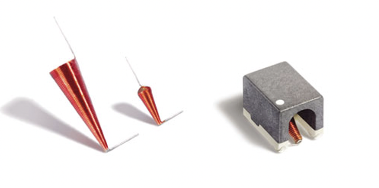
A: Clever engineers have resorted to using conical spiral inductors, which appear electrically as a stepped series of inductors for different frequencies along with steps of parasitic capacitors, as shown in Figure 2.

Figure 2. The conical inductor is a valuable addition to the “bag of tricks” used to implement a wideband boas tee; (left) the basic, somewhat fragile “flying lead” version, (right) the inductor placed in a more rugged surface-mount package. (Image: Coilcraft)
The conical shape limits the effects of stray capacitance and effectively creates a series of narrowband inductors, resulting in high impedance over a very wide bandwidth. A single conical inductor can replace a series of multiple narrowband inductors.
Note that conical inductors are not new and have been known since the “early days” — Nikolai Tesla used them in some of his designs. Volume manufacturing of these inductors in tiny sizes, however, is a modern development.
Q: Do designers have to design, model, and fabricate their bias tee units?
A: Absolutely not. Despite their simple schematic and appearance, they are complicated with many subtleties. For example, practical wide-band RF and microwave bias tees use special circuit topologies to avoid the shunt path, which would affect performance. These bias tees use a series of Inductors, additional capacitors, and resistors to prevent resonances.
Q: What are some bias-tee versions in standard use?
A: Bias tees are commercially available from dozens of vendors. Some offer a focused product range targeting a narrow class of applications. In contrast, others have an extensive portfolio of bias tees that span narrow RF bands, wideband systems, a range of power levels, and multiple package types. The bulk are surface mount or have solder pins. Connector versions include SMA female, 2.4 mm, 2.92 mm, 3.5 mm, and Type N. (Older BNC and even SO-239 connectors are also available.) Maximum voltage ratings are typically between 24 and 100 volts, while maximum DC current ranges from 200 milliamps to about 7 amps, although units outside these ranges are also available.
Q: What types of packaging are used for bias tees?
A: Packaging is a function of frequency range and power levels. Some are offered as small, shielded packages complete with RF connectors of various types, as seen in Figure 3, while others are available as tiny surface-count devices. Even when “odd” components, such as conical inductors with flying leads, are used, the complete bias tee is usually packaged in a small plastic or epoxy housing for use on a printed circuit board (PCB), just like any other surface-mount technology (SMT) device.
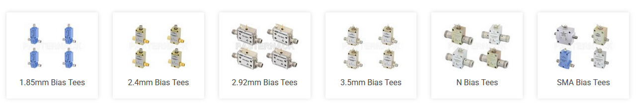
Figure 3. Commercial bias tee kits are available in a wide range of packages with different RF connectors (not shown are the surface-mount packages). (Image: Pasternack)
Many of the larger ones — those at least a few centimeters on each side, and with integral RF connectors — have their connection information printed directly on their body, as seen in Figure 4. This is in sharp contrast to the mystery associated with through-hole leaded and surface-mount ICs.
Q: What about impedance, which is always an issue in RF components?
A: Commercial vendors of bias tees offer them in both 50-ohm and 75-ohm versions to meet the needs of the two different RF application groups. Note that 50 ohms is typically used for most wireless applications, while 75 ohms is used for many video-related and legacy applications.
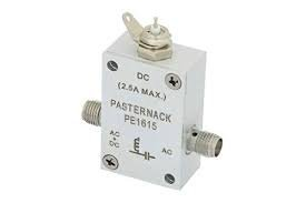
Figure 4. Many bias tee designs are large enough to be clearly marked with their schematic diagrams and connector functions. (Image: Pasternack via Quora)
Q: What parameters define the bias tee for the designer?
A: They are the ones seen for many RF components:
- Lowest RF frequency
- Upper operating frequency
- Maximum RF input current
- RF insertion loss (dB)
- DC port isolation (dB)
- Power handling on each port
- VSWR
- Package style
Summary
Bias tees provide a functionally simple yet very useful DC and RF function. As with all RF devices, the challenge is transitioning from concept to physical implementation. Vendors offer a wide range of standard units that are fully characterized across various frequency ranges, spans, power levels, and packaging options. The references have application and product information from some of these vendors.
References
RF/Microwave Bias Tees from Theory to Practice, Mini-Circuits
What is a Bias Tee?, Everything RF
Bias Tees, Spectrum Control
What is a Bias Tee Design concept?, Quora
Bias Tees (Bias Ts), Pasternack
Power-handling capabilities of inductors, Coilcraft
Solving RF Isolation Issues with RF Inductors, Coilcraft
What is a Conical Inductor?, Coilcraft
Bias Tee, Wikipedia
Related EE World Online content
What are RF inductors?
Getting one wire to do more, Part 3 – Powering the antenna LNA
What is the voltage standing wave ratio (VSWR) in RF systems?
What is a Smith chart, and why do I need one? (Part 2)
VSWR and impedance, Part 3: Implications
VSWR and impedance, Part 4: Measurements
VSWR and impedance, Part 6: Microstrip and stripline